
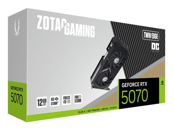
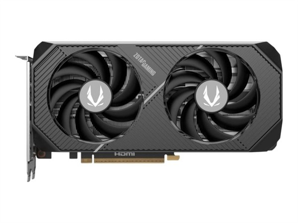


Zotac Gaming GeForce RTX 5070 Twin Edge OC/12GB GDDR7/HDMI/3x DP
Speicher: 12GB GDDR7, 192bit, 28Gbps, 1750MHz, 672GB/?s
Takt Basis: 2116MHz
Takt Boost: 2542MHz
Übertaktung: +32MHz Boost
Kühlung: 2x Axial-Lüfter (90mm) mit 0dB-Zero-Fan-Modus
TDP/TGP: 250W (NVIDIA), max. 250W (Zotac)
Stromanschlüsse: 1x 12V-2x6 (via Adapter: 2x 8-Pin PCIe)
Anschlüsse: 1x HDMI 2.1b, 3x DisplayPort 2.1b UHBR20
Anbindung: PCIe 5.0 x16
Info: Beleuchtung (RGB), Backplate, AI-Beschleunigung, NVIDIA GeForce SFF-Ready, Grafikkarten-Halterung
Gesamthöhe: Dual Slot
Abmessungen: 241.5x120.1x40.6mm (LxBxH)
Bauform: PCIe-Karte (full height)
Slotblende: full height
AI-Rechenleistung (dense): 494 TOPS (FP4), 247 TOPS (FP8), 123.5 TOPS (FP16)
AI-Rechenleistung (sparse): 988 TOPS (FP4), 494 TOPS (FP8), 247 TOPS (FP16)
GPU-Rechenleistung: 30.72 TFLOPS (FP16), 30.72 TFLOPS (FP32), 0.48 TFLOPS (FP64)
Chip-Architektur: NVIDIA Blackwell (ab 2025/?Q1)
Chip-Bezeichnung: GB205 (GB205-300-A1)
Chip-Ausbau: 96% aktive Recheneinheiten (48/?50 SM)
Chip-Konfiguration: 48SM (6144SP/?192TMU/?80ROP), 48 RT-Cores, 192 Tensor-Cores, 48MiB L2-Cache
Chip-Fertigung: TSMC N5P [NVIDIA 4N] (5nm)
Chip-Größe: 263mm², monolithisch, 31.1 Mrd. Transistoren
Chip-Funktionen: Raytracing (4th Gen NVIDIA RTX, 94 TFLOPS), NVIDIA Tensor (5th Gen, 123.5 TOPS), HDCP 2.3
Chip-Verwendung: GeForce RTX 5070 (exklusiv)
API-Unterstützung: DirectX 12 Ultimate (12_2) /? CUDA 12.8 /? Vulkan 1.3 /? OpenCL 3.0 /? OpenGL 4.6 /? Shader Model 6.8
Transcoding-Engine: 1x NVENC (9th Gen, max. Sessions: 8), 1x NVDEC (6th Gen)
Encoding: AV1 (YUV 4:2:0), H.265 (4K YUV 4:2:0 /? 4K YUV 4:2:2 /? 4K YUV 4:4:4 /? 4K Lossless /? 8K /? HEVC 10bit support /? HEVC B Frame support), H.264 (YUV 4:2:0 /? YUV 4:2:2 /? YUV 4:4:4 /? Lossless)
Decoding: AV1 (8bit /? 10bit), H.265 (8bit 4:2:0 /? 10bit 4:2:0 /? 12bit 4:2:0 /? 8bit 4:2:2 /? 10bit 4:2:2 /? 8bit 4:4:4 /? 10bit 4:4:4 /? 12bit 4:4:4), H.264 (8bit 4:2:0, 10bit 4:2:0, 8bit 4:2:2, 10bit 4:2:2), VP9 (8bit /? 10bit /? 12bit), VP8, VC-1, MPEG-2, MPEG-1
Takt Basis: 2116MHz
Takt Boost: 2542MHz
Übertaktung: +32MHz Boost
Kühlung: 2x Axial-Lüfter (90mm) mit 0dB-Zero-Fan-Modus
TDP/TGP: 250W (NVIDIA), max. 250W (Zotac)
Stromanschlüsse: 1x 12V-2x6 (via Adapter: 2x 8-Pin PCIe)
Anschlüsse: 1x HDMI 2.1b, 3x DisplayPort 2.1b UHBR20
Anbindung: PCIe 5.0 x16
Info: Beleuchtung (RGB), Backplate, AI-Beschleunigung, NVIDIA GeForce SFF-Ready, Grafikkarten-Halterung
Gesamthöhe: Dual Slot
Abmessungen: 241.5x120.1x40.6mm (LxBxH)
Bauform: PCIe-Karte (full height)
Slotblende: full height
AI-Rechenleistung (dense): 494 TOPS (FP4), 247 TOPS (FP8), 123.5 TOPS (FP16)
AI-Rechenleistung (sparse): 988 TOPS (FP4), 494 TOPS (FP8), 247 TOPS (FP16)
GPU-Rechenleistung: 30.72 TFLOPS (FP16), 30.72 TFLOPS (FP32), 0.48 TFLOPS (FP64)
Chip-Architektur: NVIDIA Blackwell (ab 2025/?Q1)
Chip-Bezeichnung: GB205 (GB205-300-A1)
Chip-Ausbau: 96% aktive Recheneinheiten (48/?50 SM)
Chip-Konfiguration: 48SM (6144SP/?192TMU/?80ROP), 48 RT-Cores, 192 Tensor-Cores, 48MiB L2-Cache
Chip-Fertigung: TSMC N5P [NVIDIA 4N] (5nm)
Chip-Größe: 263mm², monolithisch, 31.1 Mrd. Transistoren
Chip-Funktionen: Raytracing (4th Gen NVIDIA RTX, 94 TFLOPS), NVIDIA Tensor (5th Gen, 123.5 TOPS), HDCP 2.3
Chip-Verwendung: GeForce RTX 5070 (exklusiv)
API-Unterstützung: DirectX 12 Ultimate (12_2) /? CUDA 12.8 /? Vulkan 1.3 /? OpenCL 3.0 /? OpenGL 4.6 /? Shader Model 6.8
Transcoding-Engine: 1x NVENC (9th Gen, max. Sessions: 8), 1x NVDEC (6th Gen)
Encoding: AV1 (YUV 4:2:0), H.265 (4K YUV 4:2:0 /? 4K YUV 4:2:2 /? 4K YUV 4:4:4 /? 4K Lossless /? 8K /? HEVC 10bit support /? HEVC B Frame support), H.264 (YUV 4:2:0 /? YUV 4:2:2 /? YUV 4:4:4 /? Lossless)
Decoding: AV1 (8bit /? 10bit), H.265 (8bit 4:2:0 /? 10bit 4:2:0 /? 12bit 4:2:0 /? 8bit 4:2:2 /? 10bit 4:2:2 /? 8bit 4:4:4 /? 10bit 4:4:4 /? 12bit 4:4:4), H.264 (8bit 4:2:0, 10bit 4:2:0, 8bit 4:2:2, 10bit 4:2:2), VP9 (8bit /? 10bit /? 12bit), VP8, VC-1, MPEG-2, MPEG-1
